What is Skew in VLSI | Complete Guide with Examples
Table of Contents
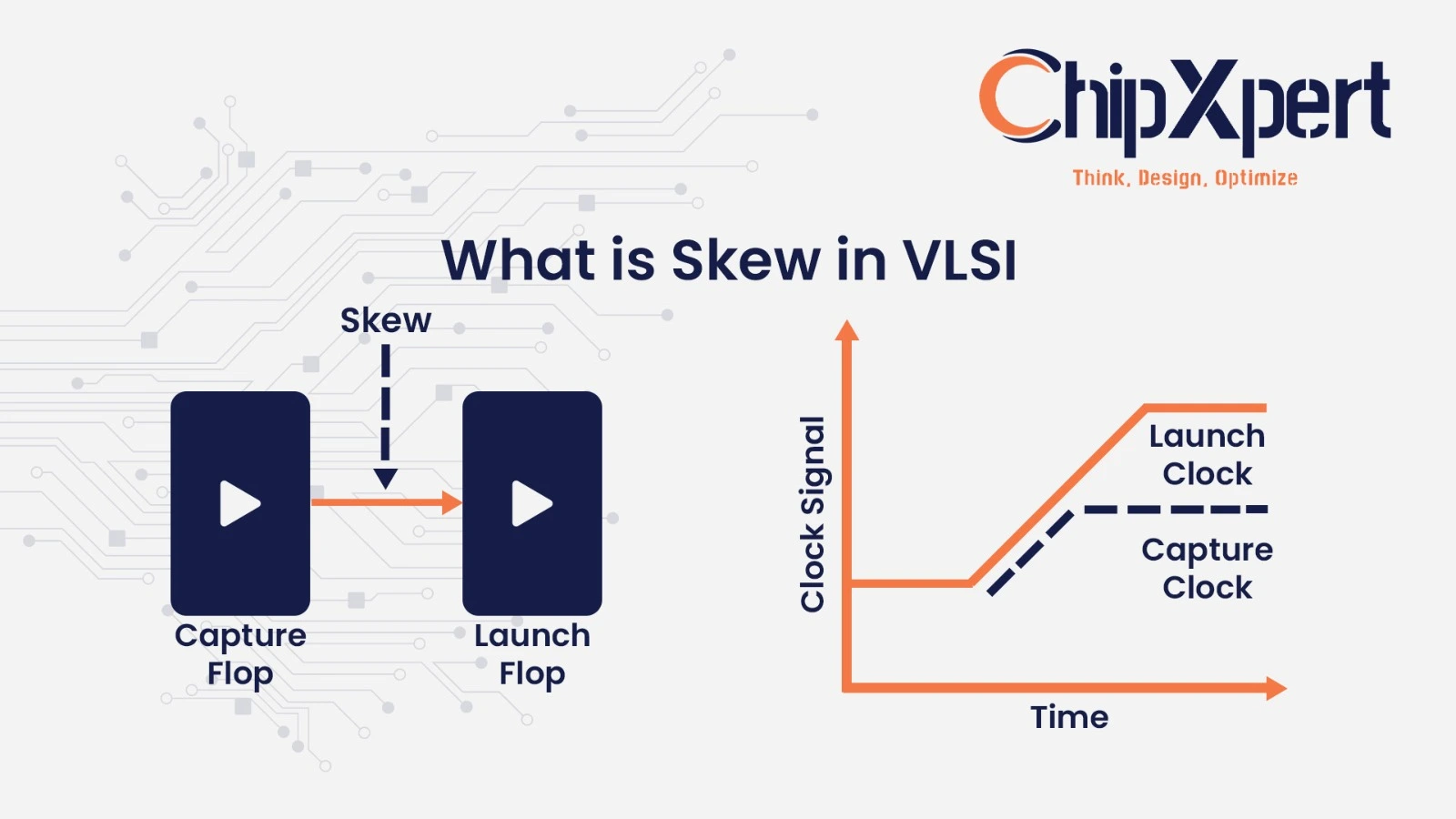
What is Skew in VLSI
When learning VLSI design, one of the most common terms you’ll hear is what is skew in VLSI. In simple words, skew happens when the signal at the clock pin of two flip flops arrives at slightly different times. This small delay can cause timing violations if not handled properly.
Understanding skew is important for physical design and making clock trees. It affects setup timing, hold time, and chip performance.
Basics of Skew in VLSI Design
Skew in VLSI design is the difference in clock arrival time at two sequential elements. For example, if one clock edge reaches the launch flop earlier than the capture clock, there will be skew.
If the skew is positive, the data path gets more time for setup. If it is negative, the design might face hold issues.
Clock Skew in VLSI
Clock skew in VLSI is simply the variation in clock arrival time across different elements. Since large chips have complex clock tree synthesis, clock edges don’t reach all flops at the same instant.
Two main types of clock skew exist:
- Positive Skew – When the capture clock arrives later than the launch clock. This helps setup timing but can cause hold problems.
- Negative Skew – When the capture clock arrives earlier. This helps hold time but can hurt setup timing.
Both need careful management to prevent timing violations.
Useful Skew in VLSI
One interesting concept is useful skew in VLSI. Instead of fighting skew, designers sometimes use it to their advantage. By deliberately adjusting clock delays, they can fix setup and hold issues.
For example:
- Adding positive skew can fix a failing setup path.
- Adding negative skew can fix a failing hold path.
Many designers widely use this method in advanced physical design flows.
Why Skew Happens in VLSI Design
Skew occurs because of multiple factors in the clock tree synthesis process, such as:
- Different wire lengths in the data path.
- Buffer insertion delays.
- Variation in clock period or clock edge arrival.
- Environmental variations like temperature and voltage.
Engineers use balanced clock trees, shielding, and optimization techniques to minimize skew.
Impact of Skew on Setup and Hold Timing
Skew has a direct impact on setup timing and hold time:
- Setup Timing: Positive skew gives more time for data to reach the capture flop.
- Hold Time: Negative skew ensures data does not arrive too early.
If you do not control skew, timing violations happen, causing functional errors. That’s why skewing is part of every design course and real-world VLSI project.
Role of Skew in Clock Tree Synthesis
During clock tree synthesis (CTS), the main goal is to distribute the clock with minimal skew. However, perfect zero skew is impossible. Instead, tools aim to:
- Balance clock delays across all flip flops.
- Optimize for both setup and hold timing.
- Control insertion delay and overall clock period.
CTS is an essential stage in physical design for assessing and correcting skew.
Skew in VLSI and Flip Flops
Skew directly affects how flip flops operate in a sequential circuit. If the clock’s arrival time changes a lot between the launch flop and the capture clock, it can cause wrong data storage.
Thus, skew impacts the data path, stability of signals, and synchronization of the overall design.
Preventing Timing Violations because of Skew
Designers use different techniques to minimize skew-related timing violations:
- Careful clock tree synthesis.
- Buffer insertion and clock balancing.
- Using useful skew strategies.
- Proper design flow with timing analyzing tools.
These methods ensure that chips run correctly at the required frequency without errors.
Why Students Must Learn Skew in VLSI
For students and engineers, understanding skew is crucial. Every VLSI design course covers it in detail because:
- Handling timing violations is essential.
- It connects concepts like setup and hold, flip flop behavior, and clock edge arrival.
- It prepares future chip designers to deal with real-world clocking challenges.
Conclusion
Now you know exactly what is skew in VLSI—the difference in clock arrival time at sequential elements. From clock skew in VLSI to useful skew in VLSI, the concept is central to chip design.
By mastering skew, you can improve setup timing. This helps you avoid hold time failures. It also ensures strong designs during physical design and clock tree synthesis.
Understanding skew is not just a theory. A practical skill that every chip designer and VLSI engineer must learn.
